Nokia 2700 full pcb diagram mother board layout. Nokia x6 full pcb diagram mother board. Nokia 220 diagram board layout pcb mother resolution high
Nokia Schematic Diagrams Download - AliSaler.com
Nokia x2 diagram layout pcb board mother resolution high repairing u2ugsm Handphone gsm cdma: nokia 5130 full pcb motherboard layout diagram Diagram nokia board pcb 2690 mother layout resolution high
Nokia 220 full pcb diagram mother board layout
Diagram board nokia c1 pcb mother layout caption samsung repairingNokia c1-01 full pcb diagram mother board layout. Nokia layout diagram x2 board pcb mother resolution high cellphoneCircuit nokia diagram phone mobile maintenance seekic electrical equipment.
Vijay mobiles kodaly: 2700Circuit board from a nokia 3310 mobile phone stock photo: 29316198 Nokia x2-02 full pcb diagram mother board layout.2700 nokia kodaly mobiles vijay pcb.

Nokia x2-02 full pcb diagram mother board layout
Nokia 2690 full pcb diagram mother board layout.Mobile phone block diagram Nokia schematic diagrams downloadNokia diagram mobile circuit.
Nokia 1280 full pcb diagram mother board layout.Nokia schematic diagram circuit phone diagrams alisaler cell below link Nokia 5110/6110 mobile phone maintenance circuit diagramNokia x6 diagram pcb board mother resolution high repairing diagrams mobile u2ugsm.

2700 nokia board pcb diagram mother layout jpgm resolution high kodaly mobiles vijay
Nokia circuit cell mobilecellphonerepairingMotherboard pcb nokia Nokia 1280 board diagram mother pcb resolution layout pc high.
.


Nokia X6 Full PCB Diagram Mother Board.

Nokia 5110/6110 mobile phone maintenance circuit diagram - Electrical
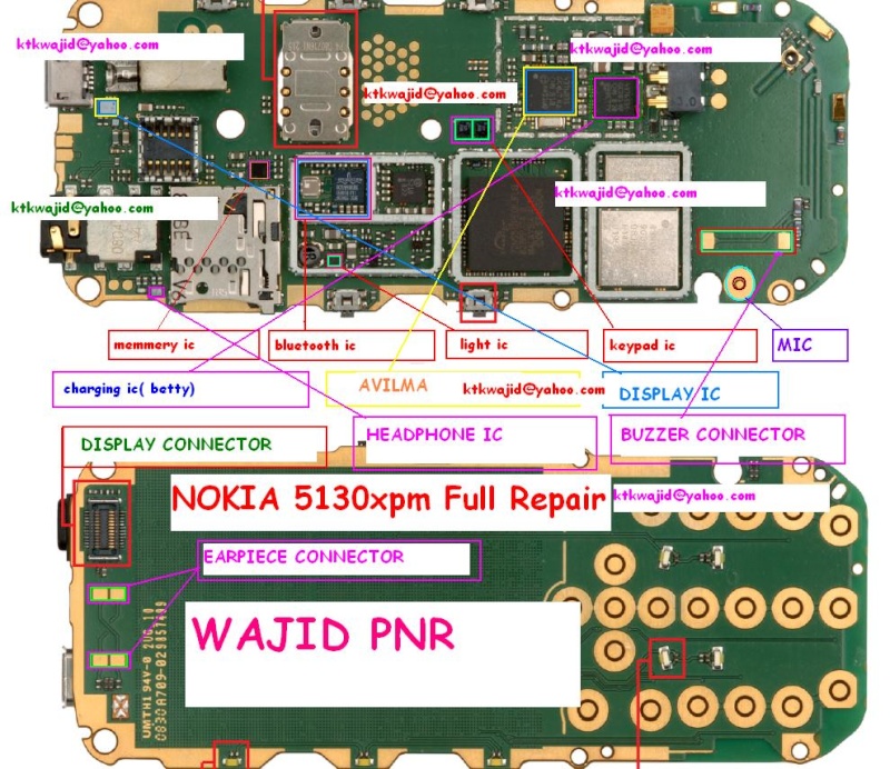
HANDPHONE GSM CDMA: Nokia 5130 Full PCB Motherboard Layout Diagram

Nokia 2690 Full PCB Diagram Mother Board Layout.

Mobile Phone Block Diagram | Nokia 3310 Block Diagram

Nokia - Download Free- All Mobile Circuit Diagram

Nokia X2-02 Full PCB Diagram Mother Board Layout

Nokia 220 Full PCB Diagram Mother Board Layout

Nokia 2700 Full PCB Diagram Mother Board Layout.
